0
Skip to Content
Columbia Nano Initiative
Welcome
History
CNI Executive Committee
Administrative Staff
Technical Staff
CNI Key Faculty
NANO-NY REU
Fellows
Contact Us
CNI Org Chart (PDF)
Overview
Badger
The CNI Labs Team
External User Program
Clean Room
Electron Microscopy
SMCL Home
New Events
Overview
CNI Grant Management
Purchasing
Travel Guidelines
Forms
Related Links
CUbiC
EFRC
MRSEC
Previous Centers
Faculty Labs
Columbia SECM Lab
The Carleton Lab
CUNY ARSC
Blog
Folder: About
Back
Welcome
History
CNI Executive Committee
Administrative Staff
Technical Staff
CNI Key Faculty
NANO-NY REU
Fellows
Contact Us
CNI Org Chart (PDF)
Folder: CNI Labs
Back
Overview
Badger
The CNI Labs Team
External User Program
Clean Room
Electron Microscopy
SMCL Home
New Events
Folder: CNI Business Office
Back
Overview
CNI Grant Management
Purchasing
Travel Guidelines
Forms
Related Links
Folder: Centers
Back
CUbiC
EFRC
MRSEC
Previous Centers
Folder: Collaborating Labs
Back
Faculty Labs
Columbia SECM Lab
The Carleton Lab
CUNY ARSC
Blog

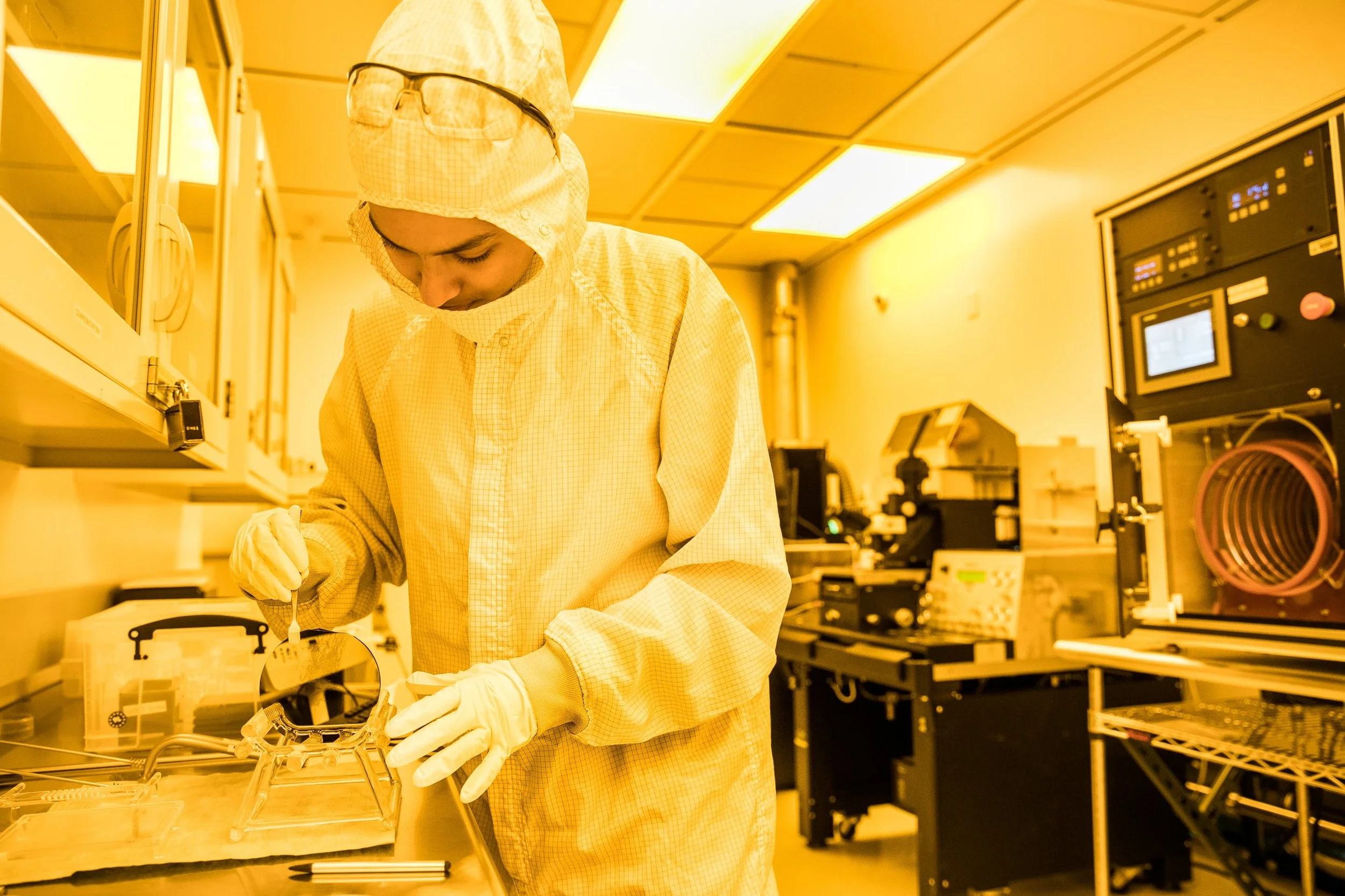
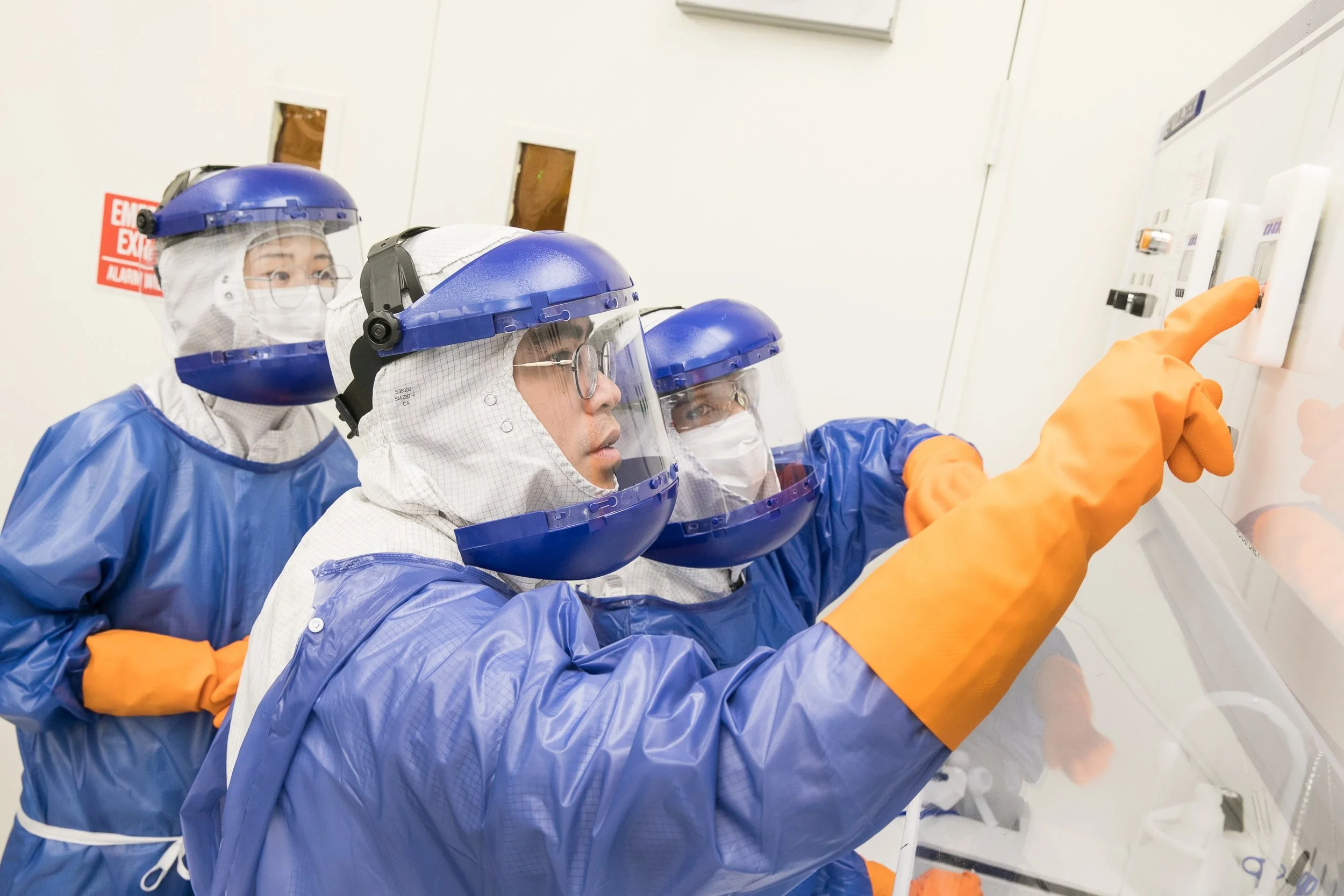
Clean Room Process & Fabrication

A great resource library for nanofabricaiton processes can be found on the UC Berkley website.

SILICON WAFERS
Silicon wafer manufacturing

THIN FILM DEPOSITION
Electron beam evaporation
Tooling factor calibration SOP
Sputtering deposition Introduction

LITHOGRAPHY
Photolithography Introduction
Spin Coating Processes

PHOTORESISTS DATA SHEETS
SPR220
AZ P4000
S1800
SU8 2000 series
PMMA
LOR
Ma-N 2400 series
ZEP

RESIST PROCESSING
PMMA SOP
LOR Photoresist Series
Photolithography Negative
SHIPLEY 1800 Series
SU8 Photoresist

ETCHING
Dry Etch Basics

DEVELOPER
AZ 300MIF Developer
AZ 400K Developer
SU8 Developer

CLEANING
RCA clean - basics
AZ 300T & 400T Stripper
Remover PG

WAFERS DICING
Dicing saw

Cleanroom user loading wafers into a quartz wafer boat in preparation for plasma ashing.
Three cleanroom users in full chemical PPE operating an acid wet bench to run a chemical cleaning process.

530 W. 120th St., Schapiro/CEPSR, MC 8903, Suite 1001 New York, NY 10027 | (212) 854-3265

© 2025 Columbia University