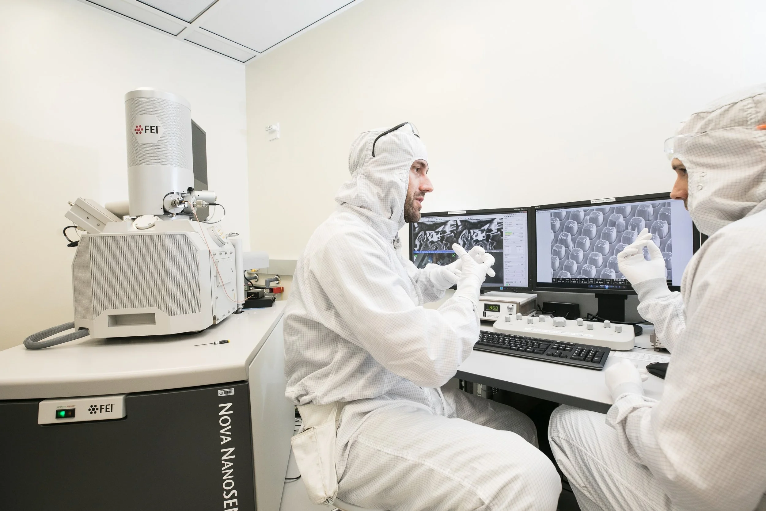
FEI NOVA NANO SEM and NPGS E-BEAM WRITER

MANUFACTURER WEBSITE | STANDARD OPERATING PROCEDURE
The FEI Nova Nano SEM (located in the clean room) uses the Nanometer Pattern Generation System for Electron Beam Lithography Writing. NPGS provides a very flexible system which is ideally suited to the wide range of applications in basic research and R&D activities. Examples of some of the structures made with NPGS include: single electron devices, quantum chaos devices, quantum dots, tunnel junctions, one and two dimensional metal wires/films, linear/circular gratings, surface acoustic wave (SAW) devices, split gate devices, as well as "larger" structures such as micromechanical devices, waveguides, and bonding pads. NPGS is well suited for use in almost any application that can be done with e-beam lithography. The primary exceptions are structures covering large areas which require the capabilities of a multi-million dollar beam writer. However, in some cases, the many advanced features of NPGS allow it to be used to fabricate structures that are more difficult to make on an expensive beam writer. A typical resolution is 250 nm and above.
PG writes a pattern by simultaneously controlling the x-y scan coils and beam blanking of the microscope. The scan coils are stepped with 16-bit voltage resolution within the field of view of the microscope and the beam is blanked as needed. Patterns can be written as a series of point exposures where the beam is blanked between exposure points, or the beam can be stepped without blanking. In either case, the dwell times are controlled with better than 0.25% timing resolution at all writing speeds. To maximize throughput, the software automatically calculates the exposure points as fast as possible, independent of the actual writing speed.
Patterns may be aligned to existing alignment marks without exposing the writing area by using the alignment program AL. An alignment pattern may have several sets of windows. For example, large windows for coarse alignment followed by smaller windows for fine alignment are very useful. Each set may have up to four user defined windows anywhere on the sample. The images of the sample areas within the windows are simultaneously displayed on the PC screen. User defined overlays are also displayed superimposed on the sample images. In the Auto-Alignment mode the overlays are controlled by the computer and are individually positioned to align with the marks on the sample using a very versatile and robust cross-correlation technique, while in the semi-automatic mode the overlays are positioned manually. Once they are aligned, the program calculates a general transformation matrix that corrects for x and y magnification errors of the microscope, as well as sample rotation and offset. Signal averaging is used to optimize the image of the alignment marks for maximum alignment accuracy. This transformation matrix is subsequently used by PG when writing the pattern to give accurate registration between lithography levels.
CONTACT INFORMATION
For additional information about the FEI E-Beam Writer, please contact the clean room staff at: cniCR@columbia.edu.
