
Nanofabrication Clean Room Facility
The CNI Nanofabrication Clean Room, located within the Morris A. Schapiro Center for Engineering and Physical Science Research (CEPSR) at Columbia University, is a state-of-the-art 5,000-square-foot facility designed to advance research in nanoscale science and engineering. It provides researchers with cutting-edge fabrication and characterization tools, technical expertise, and a collaborative team-teaching environment to foster innovation in nanotechnology.
The clean room is a hub for multidisciplinary research, bringing together experts from various academic departments, including engineering, physical sciences, chemistry, biology, and medicine. It also welcomes external collaborators from academic institutions, government labs, and industry, ranging from startups to large corporations. This collaborative environment helps bridge the gap between fundamental research and practical applications, making the CNI Nanofabrication Clean Room a strategic asset for Columbia University's leadership in nanoscale science and engineering.
By providing access to advanced tools and fostering interdisciplinary collaboration, the facility plays a critical role in pushing the boundaries of nanotechnology and its applications across diverse fields.
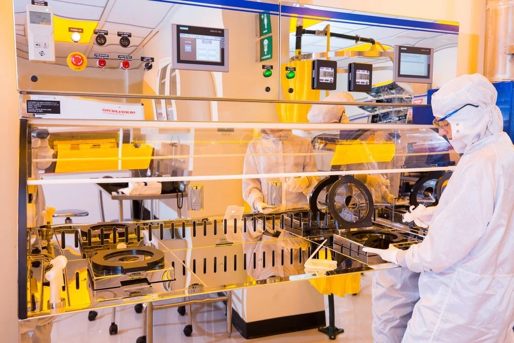
The recently-renovated and expanded CNI Nanofabrication Clean Room occupies approximately 5,000 square feet of space. It is built to be class 10,000 to class 1,000 but effectively measurements show that it is cleaner. The clean room is divided into 7 separate bays, each dedicated to a set of related fabrication processes:
Photolithography bay: includes dedicated fume hoods and photoresist spin-coaters, two mask aligners (one for DUV applications), two mask fabrication systems: a manual laser writing (3µm resolution) and an automatic laser writing system with sub-micron resolution, two plasma ashers (oxygen, argon, CF4) for substrate preparation and stock photo/e-beam resists (list of supplied resists can be found here: Supplied Resists List).
Wet chemical bay with an automatic RCA-clean bench, spin-rinse dryer for 4" wafers, general acid hood and general base hood for various wet-etch, clean and patterning processes.
E-beam lithography capability with Elionix Boden 50f and Nabity Pattern Generation System (NPGS).
Plasma bay with Reactive Ion Etching (RIE) plasma processing based on chlorine and fluorine chemistries, as well as Deep RIE for high aspect ratio and selectivity etching, and PECVD for silicon oxide, silicon nitride, and amorphous silicon deposition.
Deposition bay including two sputtering systems (dedicated to metals and dielectrics respectively) that also allow reactive sputtering, an e-beam evaporator, Ultra High Vacuum (UHV) e-beam evaporator, Atomic Layer Deposition (ALD), and a thermal evaporator (the three latter are located in the Plasma bay due to space considerations). The list of evaporation materials supplied by the clean room can be found here: Angstrom EvoVac Deposition System and Angstrom UHV E-BEAM Deposition System. The list of sputtering targets can be found here: AJA Orion 8 Dielectric Sputtering and AJA Orion 3 Metal Sputtering.
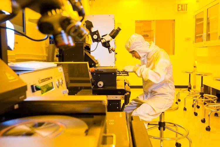
Microscopy bay consisting of a FEI Nova NanoSEM 450 (with Nabity Pattern Generation System for e-beam writing), Nikon optical microscopes (with bright/dark field and differential interference contrast), optical profilometry and two Filmetrics thin film characterization systems.
Back-end bay consisting of a Disco dicing saw, G&P chemical mechanical planarization (CMP) system, SCS Parylene coating system, Wire bonder, and a Baltec Critical Point Dryer.
Download the clean room brochure here: Clean Room Brochure.
Inventory items (wafers, wafer boxes, tweezers, notebooks, tool belts, etc.) are available to purchase from the clean room office for use in the lab. Prices are subjected to change by the actual cost of the inventory items. List can be found here: Inventory List.
Users of the lab are strongly encouraged to acknowledge CNI labs and MRSEC facilities in their publications using this recommended wording:
Cleanroom and Nanobeam users are strongly encouraged to acknowledge the use of the CNI labs and MRSEC facilities in all publications using this recommended language:
“The authors acknowledge the use of facilities and instrumentation supported by NSF through the Columbia University, Columbia Nano Initiative, and the Materials Research Science and Engineering Center DMR-2011738”
The cleanroom is open for all processes 24/7 except the corrosives bay, Cl-RIE, and the PECVD which can be used daily between 7am-9pm only.
Please sign up for the CNI Shared Lab Facilities newsletter in order to receive lab updates and important announcements by clicking here: CNI Shared Lab Facilities Newsletter
-

Jacob Trevino, PhD
Senior Director of CNI Labs
Office: 1015
Email: jt2900@columbia.edu
Phone: 212 854 9927 -

Mike Maghiar
Cleanroom Director
Office: 1020
Email: rmm2263@columbia.edu
Phone: 212 854 3032 -

Youry Borisenkov, PhD
Senior Cleanroom Engineer
Office: 1017
Email: yb2471@columbia.edu
Phone: 212 854 5688 -

Dhan Cardinal
Cleanroom Engineer
Office: 1017
Email: dc3719@columbia.edu
Phone: 212 854 1913
-

Tyson Allen
Research Operation Manager
Office: 1010
Email: ta2676@columbia.edu
Phone: 212 854 1916 here -

Hernani Pita
Chief Engineer
Office: 1017
Email: hjp2135@columbia.edu
Phone: 212 854 9143
Gallery pictures credit: Timothy Lee